- 您现在的位置:买卖IC网 > Sheet目录250 > SFCF2048H1BO2TO-I-M0-523-SMA (Swissbit NA Inc)FLASH SLC UDMA/MDMA/PIO 2G
�� �
�
�9.2.5� Bit� 3�
�This� bit� is� ‘0’.�
�9.2.6� Bit� 2� (Abort)�
�This� bit� is� set� if� the� command� has� been� aborted� because� of� a� Card� status� condition� (Not� Ready,� Write� Fault,� etc.)�
�or� when� an� invalid� command� has� been� issued.�
�9.2.7� Bit� 1�
�This� bit� is� ‘0’.�
�9.2.8� Bit� 0� (AMNF)�
�This� bit� is� set� when� there� is� a� general� error.�
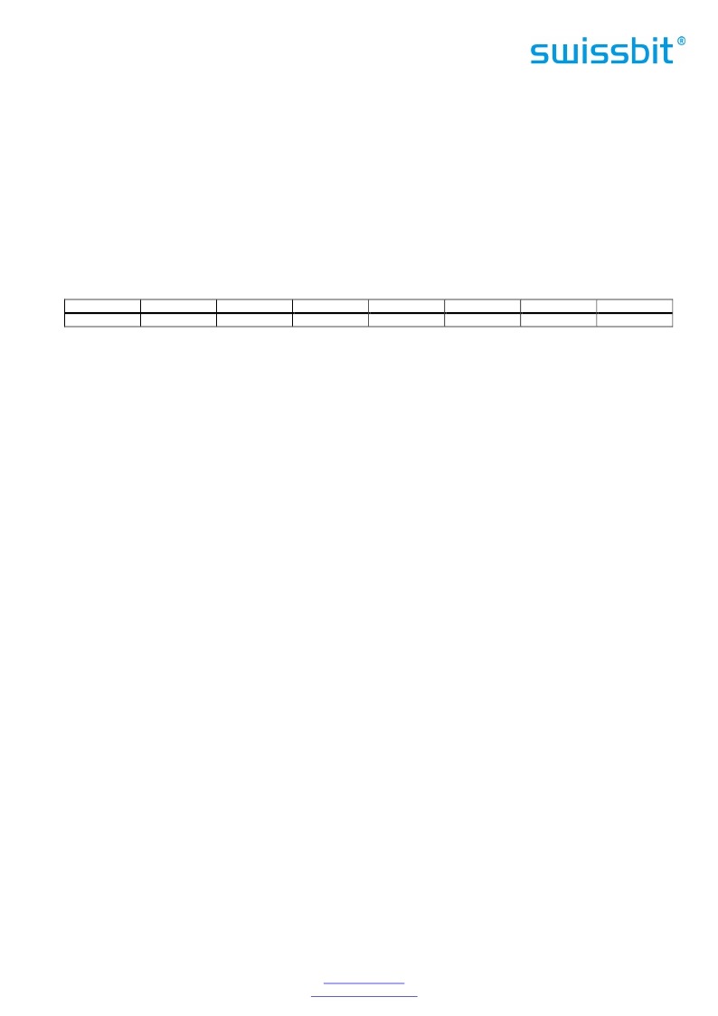
�Table 51: Error� Register�
�D7�
�BBK�
�D6�
�UNC�
�D5�
�0�
�D4�
�IDNF�
�D3�
�0�
�D2�
�ABRT�
�D1�
�0�
�D0�
�AMNF�
�9.3� Feature� Register�
�The� Feature� register� is� a� write-only� register,� located� at� address� 1F1h� [171h],� offset� 1h,� Dh.�
�This� write-only� register� provides� information� on� features� that� the� host� can� utilize.� It� is� accessed� on� data� bits� D15�
�to� D8� during� a� write� operation� to� Offset� 0� with� –� CE2� Low� and� –� CE1� High.�
�9.4� Sector� Count� Register�
�The� Sector� Count� register� is� located� at� address� 1F2h� [172h],� offset� 2h.�
�This� register� contains� the� number� of� sectors� of� data� to� be� transferred� on� a� read� or� write� operation� between� the�
�host� and� Card.� If� the� value� in� this� register� is� zero,� a� count� of� 256� sectors� is� specified.� If� the� command� was�
�successful,� this� register� is� zero� at� completion.� If� not� successfully� completed,� the� register� contains� the� number� of�
�sectors� that� need� to� be� transferred� in� order� to� complete� the� request.� The� default� value� is� 01h.�
�9.5� Sector� Number� (LBA� 7-0)� Register�
�The� Sector� Number� register� is� located� at� address� 1F3h� [173h],� offset� 3h.�
�This� register� contains� the� starting� sector� number� or� bits� 7� to� 0� of� the� Logical� Block� Address� (LBA),� for� any� data�
�access� for� the� subsequent� sector� transfer� command.�
�9.6� Cylinder� Low� (LBA� 15-8)� Register�
�The� Cylinder� Low� register� is� located� at� address� 1F4h� [174h],� offset� 4h.�
�This� register� contains� the� least� significant� 8� bits� of� the� starting� cylinder� address� or� bits� 15� to� 8� of� the� Logical� Block�
�Address.�
�9.7� Cylinder� High� (LBA� 23-16)� Register�
�The� Cylinder� High� register� is� located� at� address� 1F5h� [175h],� offset� 5h.�
�This� register� contains� the� most� significant� bits� of� the� starting� cylinder� address� or� bits� 23� to� 16� of� the� Logical� Block�
�Address.�
�9.8� Drive/Head� (LBA� 27-24)� Register�
�The� Driver/Head� register� is� located� at� address� 1F6h� [176h],� offset� 6h.�
�The� Drive/Head� register� is� used� to� select� the� drive� and� head.� It� is� also� used� to� select� LBA� addressing� instead� of�
��9.8.1� Bit� 7�
�This� bit� is� set� to� ‘1’.�
�9.8.2� Bit� 6� (LBA)�
�LBA� is� a� flag� to� select� either� Cylinder/Head/Sector� (CHS)� or� Logical� Block� Address� Mode� (LBA).� When� LBA� is� set� to� ‘0’,�
�Cylinder/Head/Sector� mode� is� selected.� When� LBA� is� set� t� o’1’,� Logical� Block� Address� is� sel� ected.� In� Logical� Block�
�Mode,� the� Logical� Block� Address� is� interpreted� as� follows:�
�Swissbit� AG�
�Industriestrasse� 4�
�Swissbit� reserves� the� right� to� change� products� or� specifications� without� notice.�
�Revision:� 1.20�
�CH-9552� Bronschhofen�
�Switzerland�
�www.swissbit.com�
�industrial@swissbit.com�
�C-320_data_sheet_CF-HxBO_Rev120.doc�
�Page� 52� of� 101�
�发布紧急采购,3分钟左右您将得到回复。
相关PDF资料
SFCF4096H4BK2SA-I-QT-553-SMA
FLASH SLC UDMA/MDMA/PIO 4G
SFCF64GBH2BU4TO-I-NU-517-STD
FLASH SLC UDMA/MDMA/PIO 64GB
SFN08B4702CBQLF7
RES ARRAY 47K OHM 7 RES 8-DFN
SFP1050-12BG
FRONT END AC/DC 1050W 12V
SFP450-12BG
PWR SUP 450W 12V 36.6A W/STANDBY
SFSD1024N1BN1TO-I-DF-151-STD
FLASH MICRO SD CARD IND S-200 1G
SFSD2048L1BN2TO-I-DF-151-STD
FLASH SECURE DGTL CARD SD 2G
SFSD4096L1BN2TO-I-Q2-141-STD
FLASH SECURE DGTL CARD SDHC 4G
相关代理商/技术参数
SFCF2048H1BO2TO-I-M0-533-ZP1
制造商:SWISSBIT NA INC 功能描述:FLASH
SFCF2048H1BO2TO-I-M0-543-SMA
制造商:SWISSBIT NA INC 功能描述:FLASH
SFCF2048H2BU2TO-C-MS-527-STD
制造商:SWISSBIT NA INC 功能描述:FLASH
SFCF2048H2BU2TO-I-MS-517-STD
功能描述:FLASH SLC UDMA/MDMA/PIO 2GB RoHS:是 类别:存储卡,模块 >> 存储器,PC 卡 系列:C-440 标准包装:30 系列:- 存储容量:8GB 存储器类型:存储卡 - Extreme III SD?
SFCF2048H2BU2TO-I-MS-527-STD
制造商:SWISSBIT NA INC 功能描述:FLASH
SFCF2048H4BK1SA-C-QT-553-SMA
制造商:SWISSBIT NA INC 功能描述:FLASH
SFCF2048H4BK1SA-I-QT-553-SMA
功能描述:FLASH SLC UDMA/MDMA/PIO 2G RoHS:是 类别:存储卡,模块 >> 存储器,PC 卡 系列:C-300 标准包装:30 系列:- 存储容量:8GB 存储器类型:存储卡 - Extreme III SD?
SFCF2048H4BK2SA-C-DS-553-SMA
制造商:SWISSBIT NA INC 功能描述:FLASH SLC UDMA/MDMA/PIO 2G